Welcome to SiSTEM Technology, your reliable sales and distribution partner specialising in the semiconductor, nanotechnology, biotechnology, and precision R&D and manufacturing sectors.
Our steadfast dedication is centred around deeply understanding the distinct challenges you face, enabling us to provide transparent and effective solutions that are not only honest but also mindful of your budget constraints.
When you choose to partner with us, you benefit from a dedicated team that consistently goes above and beyond to ensure your success. We prioritise building enduring relationships based on trust and mutual prosperity, aiming to cultivate a partnership that lasts well into the future. At every step, our goal is to deliver tailored solutions that meet your needs and contribute to the sustained growth and achievement of your objectives.
Our Solutions Include:
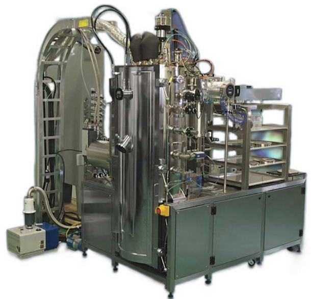
Thin Film
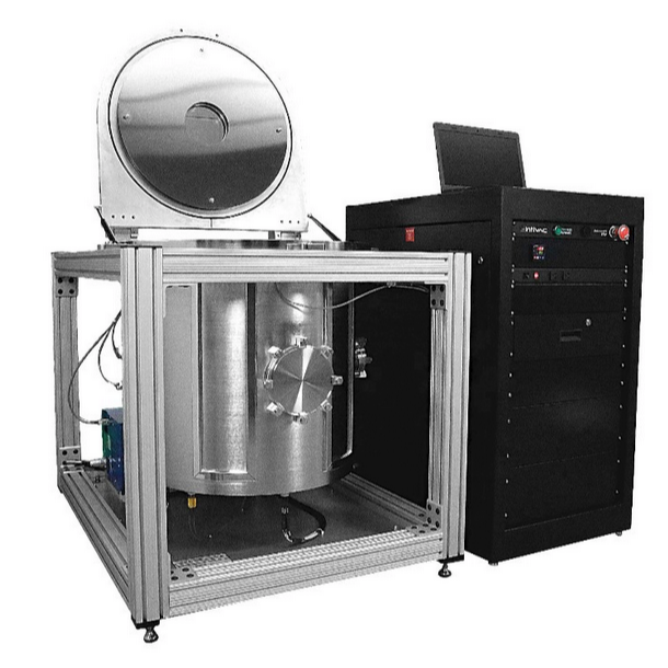
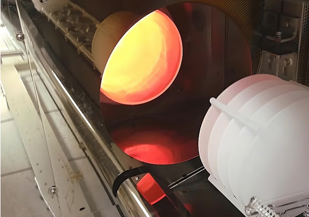
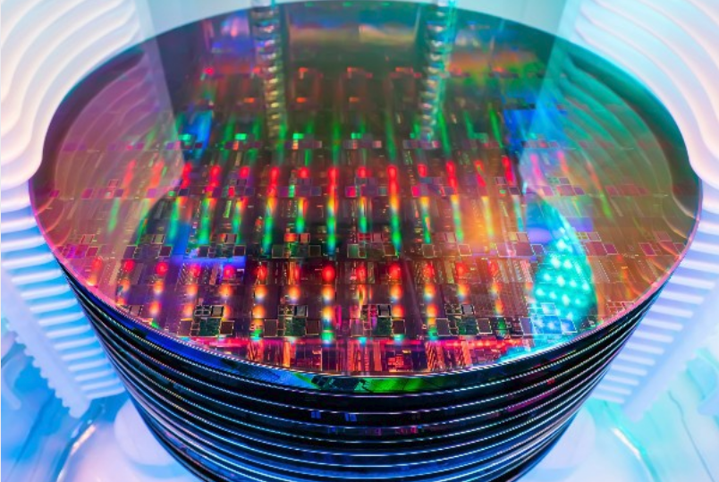
Thin film deposition equipment, utilised for physical vapor deposition (PVD), chemical vapor deposition (CVD), and atomic layer deposition (ALD), is specialised and essential for producing thin films crucial to various electronic devices like integrated circuits, solar cells, and displays.
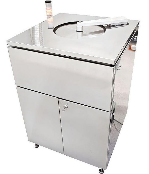
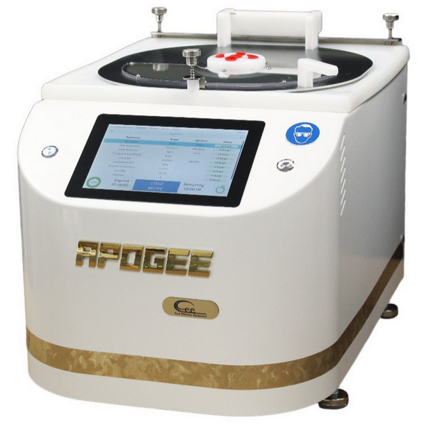
Atomic Layer Deposition
Atomic Layer Deposition (ALD) is a thin film deposition method using chemical vapor that finds extensive use across industries such as semiconductors, microelectronics, photovoltaics, and energy storage.
Ion Beam Sputter Deposition
Ion Beam Sputtering (IBS), also referred to as Ion Beam Sputter Deposition (IBSD), is a type of Physical Vapor Deposition (PVD) where an ion beam source is directed at a target to sputter atoms or molecules onto a substrate for deposition. IBS presents unique advantages and opens up a multitude of opportunities in industries such as optics, sensors (MEMS), thin film solar cells, and semiconductors.
High Precision Capillary Printing (HPCAP)
Effortlessly apply any material onto any surface with exceptional design flexibility using High Precision Capillary Printing (HPCAP). This innovative technique enables customised, localised manufacturing at micron and sub-micron scales without requiring masks, UV exposure, or chemical reactions.
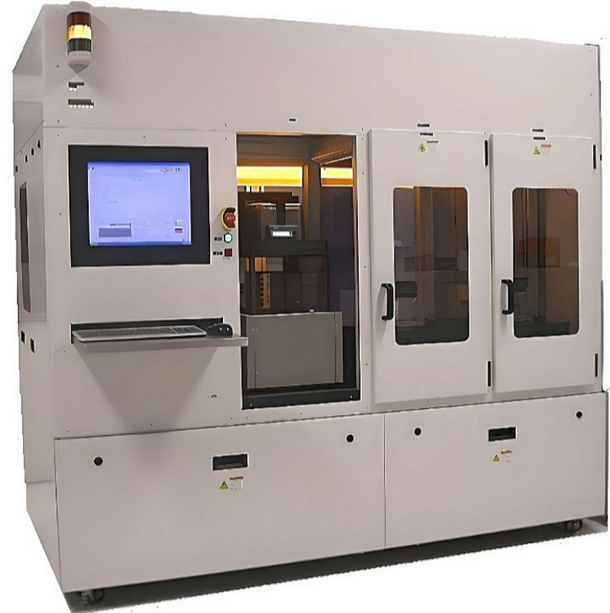
Handling & Automation
Our selection of handling and automation equipment includes various options such as retrofit open-cassette tools, SMIF pod load/unload systems, sorters, EFEMs (Equipment Front End Modules), mass wafer and reticle transfer systems, reticle storage and handling systems, as well as robots and robotic arms.
… And more.
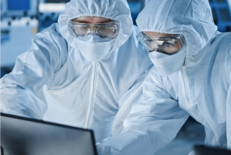
SiSTEM Technology excels in providing expertise and innovative solutions for the semiconductor, biotechnology, and nanotechnology R&D and manufacturing sectors. With extensive experience in the field, we take pride in assisting customers in their pursuit of advanced semiconductor tools. Our deep knowledge and guidance empower you to make informed decisions, driving innovation and success in this dynamic and evolving industry.
We offer tailored solutions across various industries including semiconductors, aerospace, batteries, medtech, and pharmaceuticals, addressing specific production requirements to enhance efficiency, precision, reliability, and quality in your manufacturing processes.
At SiSTEM Technology, we prioritise exceptional customer support as the cornerstone of our services. Through a customer-centric approach, we provide unparalleled assistance, ensuring your complete satisfaction.
-
-
-
-
-
-
-
-
-
-
-
-
-
-
-
-
")
Atomic Layer Deposition (ALD)

Thin Film Deposition

Reticle & Wafer Handling & Automation

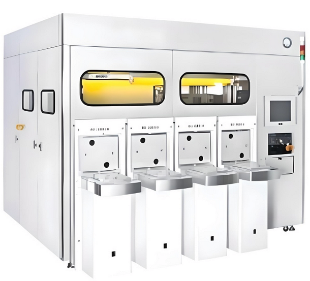
Wafer Processing Equipment

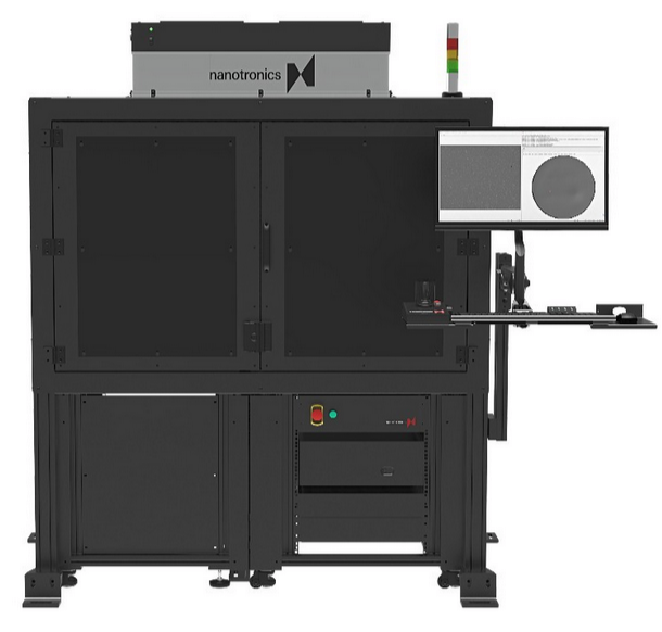
Optical Defect Inspection

Reliability Testing

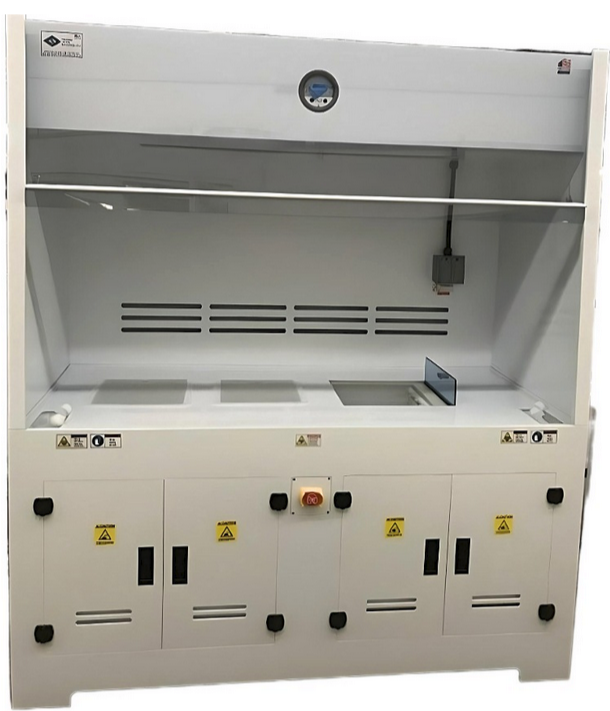
Wet Processing

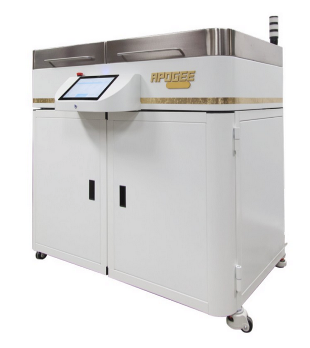
Temporary Wafer Bond & Debond Tools

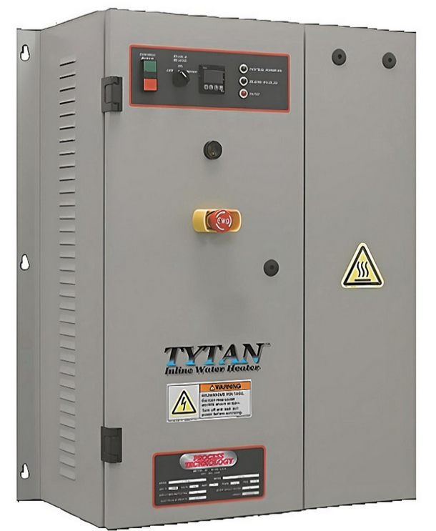
Water & Chemical Heaters

Thermal Processing
")
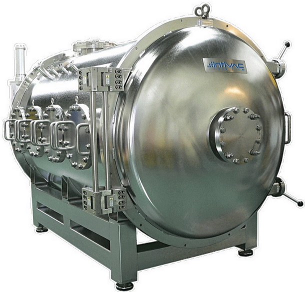
Thermal Vacuum (TVAC)

Megasonics

Degassing Systems

Probe, Test & Burn-In

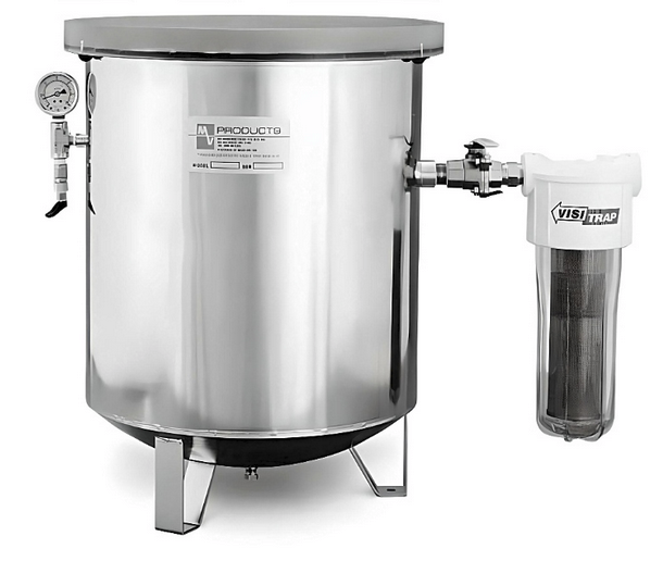
Vacuum Chambers, Traps & Consumables

Chuck Cleaning Wafers
Previous
Next

 approvedbusiness.co.ukSiSTEM Technology Tel: 01327 362844